Explore Semiconductor Equipment Manufacturing: Guide to Lithography, Etching, and Fabrication Systems
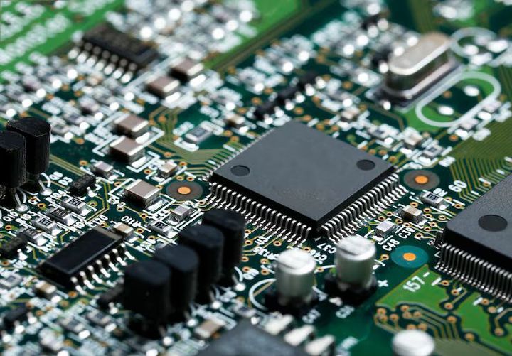
Semiconductor equipment manufacturing refers to the design and production of advanced machines used to create microchips. These machines perform highly precise steps such as lithography, etching, deposition, and inspection. Microchips power modern electronics including smartphones, computers, medical devices, vehicles, and communication networks.
The semiconductor industry exists because electronic devices require increasingly smaller, faster, and more energy-efficient components. To achieve this, manufacturers use specialized wafer fabrication technology inside controlled cleanroom environments. Semiconductor equipment manufacturing supports this ecosystem by building the systems that make microelectronics production possible.
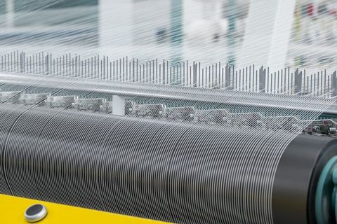
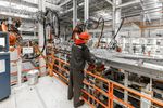
Modern fabrication facilities, often called fabs, rely on automated industrial automation systems that operate with extreme precision. A single semiconductor wafer may go through hundreds of processing steps before becoming finished integrated circuits.
Understanding Lithography, Etching, and Fabrication Systems
Lithography systems are among the most critical tools in the chip manufacturing process. They use light to transfer circuit patterns onto silicon wafers. The process involves:
-
Coating the wafer with photoresist material
-
Exposing it to patterned light
-
Developing the pattern to reveal circuit designs
Extreme Ultraviolet (EUV) lithography represents one of the most advanced forms of patterning. It enables extremely small transistor structures required for advanced semiconductor fabrication.
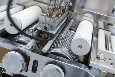
Etching systems remove material from the wafer to create precise structures. Plasma etching equipment uses reactive gases to selectively remove layers according to circuit patterns. This step shapes microscopic features that determine chip performance.
Deposition systems add thin films of materials onto wafers. These films may include conductive, insulating, or semiconductor layers.
Inspection and metrology tools measure dimensions at the nanometer scale. These systems ensure that each layer meets strict quality standards.
Below is a simplified overview of major semiconductor fabrication equipment:
| Equipment Type | Function | Example Output |
|---|---|---|
| Lithography Systems | Pattern transfer using light | Circuit layouts |
| Plasma Etching Equipment | Material removal | Transistor channels |
| Deposition Systems | Layer formation | Thin films |
| Ion Implantation Tools | Doping silicon | Electrical properties |
| Metrology Systems | Measurement & inspection | Process accuracy |
Each system must operate in highly controlled cleanroom technology environments to prevent contamination.
Why Semiconductor Equipment Manufacturing Matters Today
Semiconductor equipment manufacturing is central to the global semiconductor supply chain. As digital transformation accelerates, demand for chips continues to grow across industries.
Key sectors affected include:
-
Consumer electronics
-
Automotive systems and electric vehicles
-
Artificial intelligence and data centers
-
Healthcare equipment
-
Telecommunications and 5G networks
Advanced semiconductor fabrication enables smaller transistors, which improve computing speed and energy efficiency. This directly affects battery life in devices, performance in AI systems, and reliability in industrial automation systems.
The sector also addresses challenges such as:
-
Rising global demand for microchips
-
Supply chain resilience
-
Technological competitiveness among nations
-
Energy efficiency improvements
Semiconductor equipment manufacturing contributes to innovation by enabling next-generation chips used in artificial intelligence, high-performance computing, and smart infrastructure.
Recent Updates and Trends in 2025
In 2025, semiconductor equipment manufacturing continues evolving rapidly.
In early 2025, global reports highlighted increased investment in advanced semiconductor fabrication facilities in regions such as the United States, Europe, India, Japan, and South Korea. These expansions aim to strengthen domestic production capacity and reduce supply chain risks identified in previous years.
In March 2025, industry updates indicated progress in High-NA EUV lithography systems. These next-generation lithography systems enable even smaller circuit patterns and support sub-2 nanometer technology nodes.
Artificial intelligence integration into wafer fabrication technology has also expanded in 2025. Machine learning algorithms are increasingly used to optimize plasma etching equipment performance and detect defects in real time.
Another notable trend involves energy-efficient cleanroom technology. Fabrication facilities are implementing systems that reduce power consumption and water usage while maintaining strict environmental standards.
Throughout 2024 and into 2025, semiconductor supply chain strategies have shifted toward regional diversification. Equipment manufacturers are collaborating with research institutions to accelerate innovation in materials science and microelectronics production systems.
Laws and Policies Affecting Semiconductor Equipment Manufacturing
Government policies strongly influence semiconductor equipment manufacturing due to its strategic importance.
In the United States, the CHIPS and Science Act continues to support semiconductor research and domestic fabrication expansion. Funding programs encourage advanced semiconductor fabrication and innovation in wafer fabrication technology.
The European Union’s Chips Act supports regional manufacturing capacity and research initiatives. The policy framework promotes technological sovereignty and strengthens the semiconductor supply chain within member states.
India has expanded semiconductor incentive programs to attract fabrication and equipment manufacturing investment. National electronics policies encourage infrastructure development and cleanroom technology expansion.
Japan and South Korea maintain long-term industrial strategies supporting microelectronics production systems. These programs emphasize research collaboration, export regulations, and strategic technology development.
Export control regulations also play a role in semiconductor equipment manufacturing. Certain advanced lithography systems and plasma etching equipment are subject to international trade controls to protect national security interests.
Environmental regulations further affect fabrication systems. Cleanroom operations must comply with:
-
Chemical handling standards
-
Water usage management policies
-
Emission reduction requirements
-
Waste disposal guidelines
Compliance ensures sustainable and responsible manufacturing practices.
Tools and Resources for Learning and Evaluation
Several tools and educational platforms help individuals understand semiconductor equipment manufacturing.
Technical and educational resources include:
-
Semiconductor research journals and academic publications
-
Online semiconductor fabrication courses
-
Cleanroom design simulation software
-
Process modeling tools for plasma etching equipment
-
Lithography simulation programs
Industry organizations provide white papers, technical standards, and data on microelectronics production systems.
Government portals publish semiconductor policy documents, funding guidelines, and compliance frameworks related to advanced semiconductor fabrication.
Engineering students and professionals often use:
-
CAD tools for chip layout design
-
Process control analytics software
-
Yield analysis calculators
-
Materials science databases
These resources support knowledge development in wafer fabrication technology and semiconductor supply chain management.
Frequently Asked Questions
What is semiconductor equipment manufacturing?
It refers to the production of specialized machines used to fabricate microchips. These machines perform processes such as lithography, etching, deposition, and inspection inside controlled environments.
Why is lithography important in chip manufacturing?
Lithography systems transfer microscopic circuit patterns onto silicon wafers. This step defines the size and arrangement of transistors, directly influencing chip performance and efficiency.
What does plasma etching equipment do?
Plasma etching equipment removes material from the wafer surface using reactive gases. It creates precise structures required for transistors and interconnections.
Why are cleanrooms necessary in fabrication facilities?
Cleanroom technology minimizes contamination from dust or particles. Even microscopic impurities can damage circuits at nanometer scales.
How do government policies impact semiconductor equipment manufacturing?
Policies influence research funding, infrastructure development, export controls, environmental compliance, and semiconductor supply chain strategies.
Conclusion
Semiconductor equipment manufacturing forms the backbone of modern microelectronics production. Lithography systems, plasma etching equipment, and wafer fabrication technology work together to produce increasingly smaller and more powerful chips.
In 2025, advancements such as High-NA EUV lithography and AI-driven process optimization highlight the sector’s ongoing evolution. Government policies, supply chain diversification, and environmental regulations continue shaping industry development.
As demand for digital technologies expands across industries, semiconductor equipment manufacturing remains essential for enabling innovation in computing, telecommunications, healthcare, and industrial automation systems. Understanding its processes, tools, and regulatory environment provides valuable insight into how modern electronic devices are made and how the global semiconductor supply chain continues to adapt to technological and economic changes.